Research · Jun 2024 – Oct 2025
Automated photoreactors for chemical research
ICIQ, Lloret-Fillol group
A high-power parallel photoreactor (1.2 kW at 450 nm) with a custom ESP32 + STM32F4 motherboard (PCB and firmware), embedded control, sensing, a touchscreen HMI and web and Android interfaces.
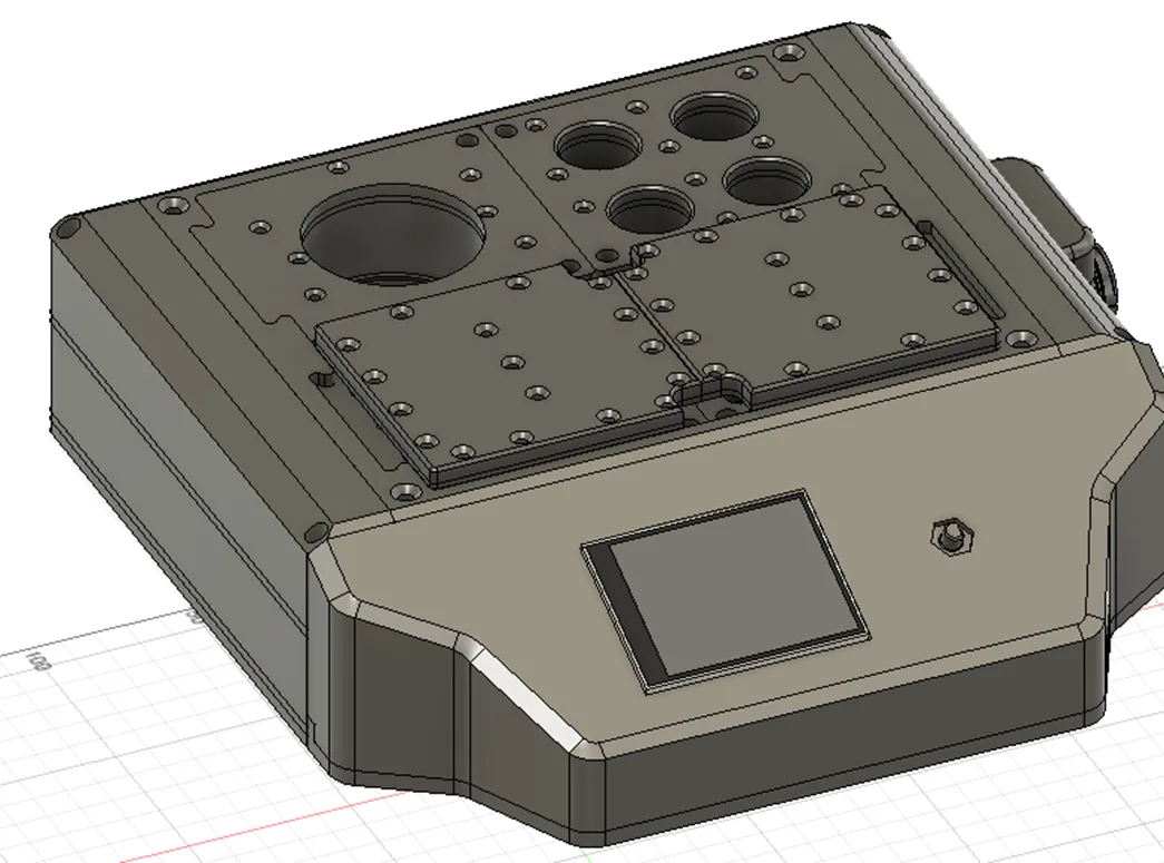
Innovative parallel photoreactor#
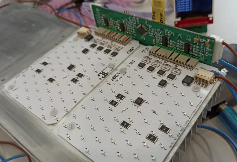
This project focuses on the development of a photoreactor with homogeneous light and high power density: up to 1.2 kW of 450 nm light (using RUBIX LEDs), built from 4 modules of 64 LEDs with 4 independent channels per module. The square photoreactor is designed primarily for photochemical research, in both synthesis and dynamics, and its high power density opens interesting applications in fine chemistry.
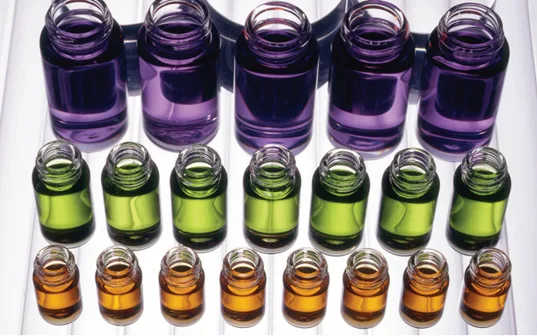
The prototype accepts four glass-vial formats:
- up to 256 × 1 mL vials
- 16 × 100 mL vials
- 4 × 500 mL vials
- 1 × 1000 mL vial
Electronics: a two-board system#
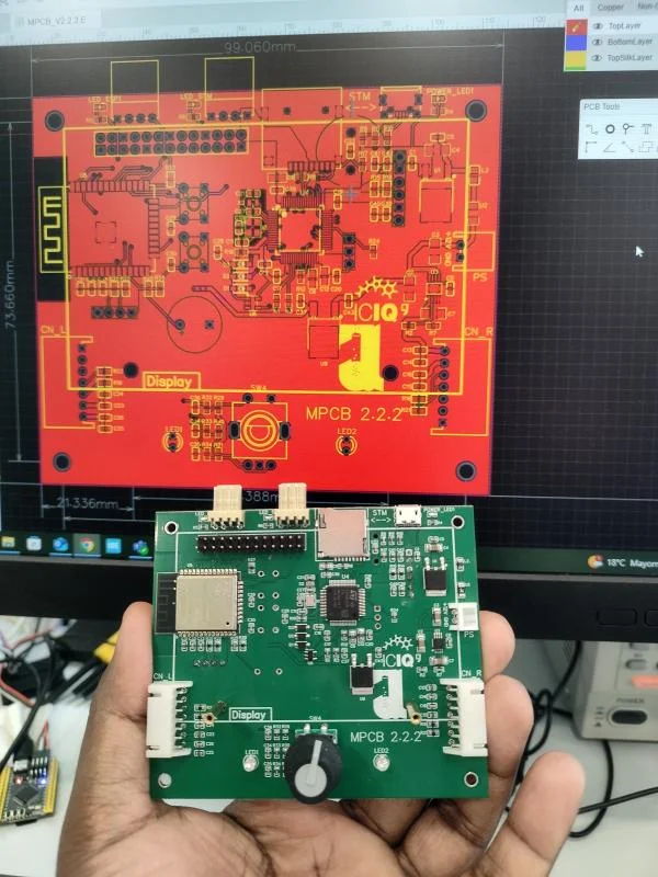
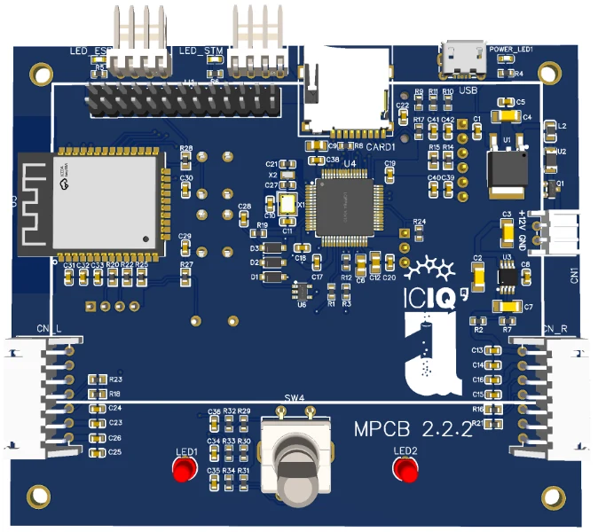
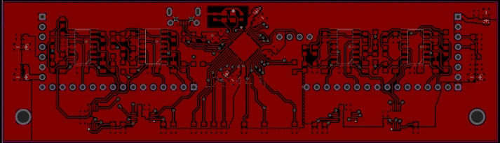
I was the lead PCB and embedded systems engineer for the photoreactor's electronics, from schematic and component selection to layout, bring-up and firmware. Both boards were designed in EasyEDA as 4-layer PCBs.
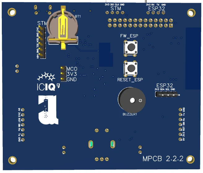
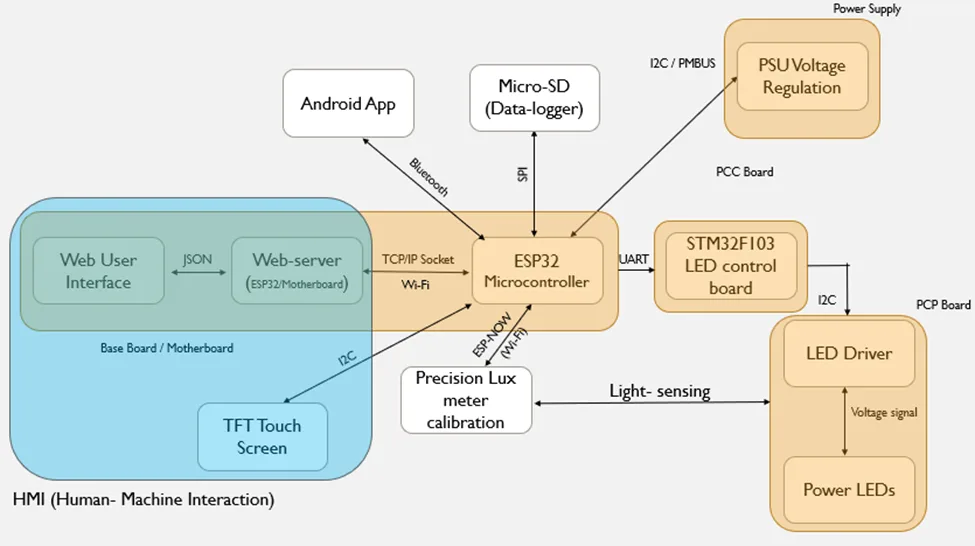
- MPCB 2.2.2 (motherboard): the central control unit. An STM32F412 runs the system and data exchange, and an ESP32 adds Wi-Fi and Bluetooth for remote monitoring. It regulates 12 V down to 9 V and 3.3 V, and links the boards over I²C, UART, SPI and USB, with a rotary encoder and status LEDs for local control.
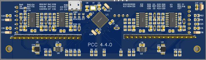
- PCC 4.4.0 (peripheral control card): the analog side. An STM32F401 drives 8 op-amp channels for the MOSFET LED drivers, sets currents through an MCP4728 DAC and measures them with an ADS1015 ADC.
| Layer | Function |
|---|---|
| Top | High-speed signals, power and main components |
| Inner 1 | Power plane (3.3 V, 9 V) |
| Inner 2 | Ground plane for EMI shielding |
| Bottom | Secondary routing, low-speed signals and connectors |
Design challenges#
- Heat: the regulators ran hot, so I added thermal vias, ground-plane heat spreading and copper pours.
- Signal integrity and EMI: USB, I²C and SPI lines picked up noise, solved with shielded USB differential pairs, shorter high-speed traces and ground-plane isolation.
- Wi-Fi interference: a dedicated RF keep-out zone and ground separation around the ESP32 antenna.
- Clock stability: crystal load capacitors calculated from C_L = (C1·C2)/(C1+C2) + C_stray, with a keep-out area under the crystal and MCU.
- Programming access: SWD headers for the STM32 and reset and boot buttons for the ESP32.
The boards were validated with power-on and current-draw tests, continuity and signal-integrity checks, firmware flashing, wireless tests, thermal monitoring and DAC/ADC calibration.
As Research Software Engineer at ICIQ (2024–2025), my work covered the embedded side: the 4-layer ESP32 + STM32F4 motherboard (PCB design and firmware), LED drivers, light sensing and calibration, a touchscreen HMI, a web interface and an Android app.
Related software: motherboard firmware (STM32F412).
Prof. Julio Lloret-Fillol Research Group, ICIQ, Tarragona, Spain.
Figures